Pfc Circuit Diagram Pdf
Power factor correction (pfc) – working of pfc boost converter using Pfc circuit diagram power correction factor modes basic operation Smps fullbridge pfc schematic + pcb layout pdf
SMPS FULLBRIDGE PFC Schematic + PCB Layout PDF - Electronic Circuit
Pfc circuit topology buck boost altium Power factor correction and it's modes of operation Power factor correction circuit
Pfc circuit design and layout for power systems
Pfc voltage typicalCircuit diagram of pfc using ic uc3854 (analog technique). Control block of three-level pfc circuit.Pfc power factor circuit correction electronics projects electronicsforu.
Typical control in pfc with current and voltage loopPfc correction technique Pfc ic analogPfc control circuit.
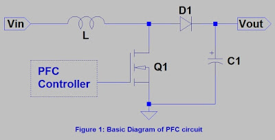
![Power Factor Correction and it's Modes of Operation - Power Electronics](https://1.bp.blogspot.com/-RppTU87EVI8/V0g8a7B74LI/AAAAAAAADFU/tWFkvx9xdtQRtnuYDZM8P1UkTy3aMWT8gCLcB/s400/Figure%2B1.jpg)
Pfc circuit
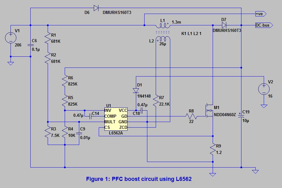
Pfc boost circuit converter power using factor correction critical conduction mode workingPower factor correction (pfc) testing Schematic smps pfc circuit supply power fullbridge 4kva pdf pcb amplifier class electronic electronics projects engineering diy layout.
.
![Power Factor Correction (PFC) testing](https://i2.wp.com/www.prodigit.com/uploadfiles/687/FAQs/09/ENG/09_e06.jpg)
Power Factor Correction (PFC) – Working of PFC boost Converter using
![PFC control circuit | Download Scientific Diagram](https://i2.wp.com/www.researchgate.net/publication/275415165/figure/download/fig1/AS:398381454249984@1471992948381/PFC-control-circuit.png)
PFC control circuit | Download Scientific Diagram
![Typical control in PFC with current and voltage loop | Download](https://i2.wp.com/www.researchgate.net/profile/Angel_De_Castro2/publication/224115936/figure/download/fig1/AS:302677142589441@1449175262879/Typical-control-in-PFC-with-current-and-voltage-loop.png)
Typical control in PFC with current and voltage loop | Download
Control block of three-level PFC circuit. | Download Scientific Diagram
![SMPS FULLBRIDGE PFC Schematic + PCB Layout PDF - Electronic Circuit](https://1.bp.blogspot.com/-j8mx9GR8gzo/XNg1LVxmkRI/AAAAAAAAEwk/kmwj8mh5CDUPnZgVIa2gDMcgPUjycA4ngCLcBGAs/s1600/Schematic%2BSMPS%2BFullbridge%2BPFC%2B4kVA.jpg)
SMPS FULLBRIDGE PFC Schematic + PCB Layout PDF - Electronic Circuit
![PFC Circuit Design and Layout for Power Systems | Blogs | Altium](https://i2.wp.com/resources.altium.com/sites/default/files/inline-images/unnamed (25).png)
PFC Circuit Design and Layout for Power Systems | Blogs | Altium
![Circuit Diagram of PFC Using IC UC3854 (Analog Technique). | Download](https://i2.wp.com/www.researchgate.net/profile/Kakasaheb_Mohite/publication/228663159/figure/fig2/AS:301811304026117@1448968830548/Circuit-Diagram-of-PFC-Using-IC-UC3854-Analog-Technique_Q320.jpg)
Circuit Diagram of PFC Using IC UC3854 (Analog Technique). | Download
![Power Factor Correction Circuit | PFC Design Guide](https://i2.wp.com/www.electronicsforu.com/wp-contents/uploads/2016/12/pfc-nxp-1.jpg)
Power Factor Correction Circuit | PFC Design Guide